Notre Dame opens new Wideband Test Facility

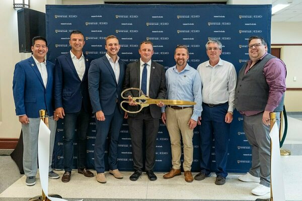
On Wednesday (August 6), the doors of the new Wideband Test Facility at the University of Notre Dame (South Bend, Indiana, USA) were officially opened to researchers and industry partners. The test facility is the latest addition to the University’s existing facilities for microelectronics development and testing, which include state-of-the-art nanofabrication and integrated imaging facilities.
“The addition of this unique antenna characterization and testing facility for microelectronics here on Notre Dame’s campus allows us to extend the impact of our faculty, staff, and student researchers,” said Jeffrey F. Rhoads, the John and Catherine Martin Family Vice President for Research and professor in the Department of Aerospace and Mechanical Engineering. “There is no doubt in my mind that this will have a direct and tangible impact in microelectronics development, which is so critical here in the Midwest and in the nation writ large.”
The Wideband Test Facility houses specialized equipment for testing electronic devices such as ultra-fast transistors as well as antennas that operate at high frequencies. It was established to address critical gaps in prototyping, as well as characterization capabilities for high-frequency wireless and sensing systems. A full-time engineer will staff the facility to assist users in testing their technology.

Notre Dame is one of four university members of the Silicon Crossroads Microelectronics Commons (SCMC) Hub, a three-state coalition formed to accelerate the expansion of America’s microelectronics base. This group of four institutions coordinates to align university resources and dedicated personnel with technical projects and the needs of the high-tech industry. The new Wideband Test Facility leverages supplemental funding from the SCMC Hub, as well as Notre Dame's existing expertise in high-performance, high-frequency electronics and antennas, to host collaborative research and development among academic, industry, and government entities.
U.S. Congressman Rudy Yakym said, “When I think of the University of Notre Dame, I think of leadership. Today, I think especially of leadership in microelectronics. A new wave of innovations is taking place right here on campus, with advanced engineering made possible by the advanced capabilities of the Wideband Test Facility.” Yakym, who represents Indiana’s Second Congressional District, added, "Such expertise will allow our country to stay on the leading edge of microelectronics development, now and in the future.”
High-frequency device testing assesses the performance of nanometer-scale semiconductor components, which are essential elements of everything from high-end computer chips, to wireless communication systems, and radar and sensing systems. The new facility enables testing with high-speed signals up to 220 Gigahertz (GHz). The ability to test chips at such high frequencies allows for the development of more efficient and reliable device components with unmatched performance.
Advanced antenna measurements are enabled by the facility’s spherical near field scanning capabilities, supporting both on-chip and antenna-in-package testing. This, coupled with a test area surrounded by anechoic foam to minimize external interferences, allows for the accurate measurement of the sending and receiving of signals by antennas, especially small ones, at frequencies from 4 GHz up to 220 GHz.

The demand for faster, more reliable, and secure wireless communication continues to grow across the globe. Technologies such as 5G, 6G, advanced radar, and high-speed satellite internet depend on electronics and antennas that operate at increasingly higher frequencies. The capabilities of the Wideband Test Facility address gaps in the ability to test devices and validate prototypes in emerging ultra-high frequency bands for these and other applications. The facility’s opening also increases the region’s capacity for testing, tech transfer, and prototyping, relieving bottlenecks in the technology development workflow.
“The capabilities of the Wideband Test Facility are game-changing for the development of high-tech electronics and wireless systems,” said Patrick Fay, Stinson Professor of Nanotechnology in the Department of Electrical Engineering. “With applications for both commercial and defense sectors, the characterization capabilities offered here are unmatched. We look forward to advancing cutting edge microelectronics technologies in collaboration with academic, industry, and government partners.”
Learn more about Notre Dame and the CHIPS and Science Act.
Contact
Erin Fennessy / Writing Program Manager
Notre Dame Research / University of Notre Dame
efenness@nd.edu / research.nd.edu
About Notre Dame Research
The University of Notre Dame is a private research and teaching university inspired by its Catholic mission. Located in South Bend, Indiana, its researchers are advancing human understanding through research, scholarship, education, and creative endeavor in order to be a repository for knowledge and a powerful means for doing good in the world. For more information, please see NDR's website or NDR's LinkedIn.
Latest Research
- NSF Cyber SMART’s fall meeting shapes fifth year of project, legacy and future plans, and adds new memberThe U.S. National Science Foundation (NSF) Cyber SMART center gathered for its fall meeting on the University of Notre Dame campus this September. The meeting served as a checkpoint with progress reports and new projects from research leads and students…
- Slavic and Eurasian studies professor wins Humboldt fellowship to research how Russia’s religious past shapes its presentWhen Russia invaded Ukraine on Feb. 24, 2022, Sean Griffin realized his second book needed a new title. Griffin, an associate professor in the University of Notre Dame’s Department of…
- Notre Dame’s R.I.S.E. AI Conference builds interdisciplinary collaboration to inform human-centered artificial intelligenceAs artificial intelligence (AI) transforms nearly every sector of society — from healthcare and education to governance and global development — a critical question emerges: How can we conscientiously design and deploy these powerful technologies to positively impact society? This…
- University of Notre Dame joins the Global Coalition of Ukrainian StudiesThe University of Notre Dame has joined the Global Coalition of Ukrainian Studies after signing a Memorandum of Cooperation (MOC), formalized on September 24, 2025, at the Ukrainian Institute of America in New York City. Notre Dame joined four other American…
- The University of Notre Dame’s Mendoza College of Business and Industry Labs team up to inspire national security manufacturing competitiveness in the regionThe South Bend - Elkhart Region is full of manufacturing companies that are poised to grow, and Executive Master of Business Administration (EMBA) and Master of Business Administration (MBA) students at the University of Notre Dame are finding innovative ways to contribute to that growth. Earlier…
- Notre Dame research informs WHO conditional recommendation for spatial repellents in malaria vector controlThe World Health Organization (WHO) recently announced a “conditional recommendation” for spatial emanators, also known as “spatial repellents,” in the fight against malaria. This key determination was informed by spatial repellent studies that included the Advancing Evidence for the Global Implementation of Spatial Repellents (AEGIS) Project in Kenya, led by the University of Notre Dame and funded by Unitaid. The findings from this particular study were recently published in The Lancet.


